


0 reviews
Be the first to review this item!

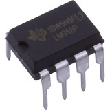
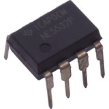
| CMRR - Common Mode Rejection Ratio | 100 dB |
| GBP - Gain Bandwidth Product | 5 MHz |
| Ib - Input Bias Current | 200 pA |
| In - Input Noise Current Density | 0.01 pA/sqrt Hz |
| Maximum Dual Supply Voltage | +/- 18 V |
| Maximum Operating Temperature | + 70 C |
| Minimum Dual Supply Voltage | +/- 5 V |
| Minimum Operating Temperature | 0 C |
| Number of Channels | 1 Channel |
| Operating Supply Current | 5 mA |
| Operating Supply Voltage | 10 V to 36 V, +/- 5 V to +/- 18 V |
| Output Current per Channel | 25 mA |
| PSRR - Power Supply Rejection Ratio | 80 dB |
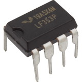
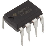
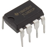
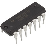
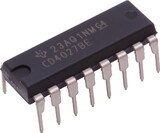
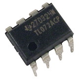
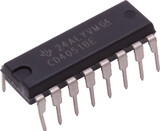
| Package | PDIP-8 |
| Pd - Power Dissipation | 670 mW |
| SR - Slew Rate | 12 V/us |
| Supply Voltage - Max | 44 V |
| Supply Voltage - Min | 10 V |
| Vcm - Common Mode Voltage | 10 V to 36 V |
| Voltage Gain dB | 106.02 dB |
| Vos - Input Offset Voltage | 2 mV |
| en - Input Voltage Noise Density | 12 nV/sqrt Hz |
| Packaging Dimensions | 0.382 in. X 0.32 in. X 0.28 in. |
| Weight (Packaging) | 0.0024 lbs. |
 Attention CA Residents: Prop 65 Warning
WARNING:
This product can expose you to chemicals which are known to the State of California to cause cancer, birth defects, or other reproductive harm. For more information, go to www.p65warnings.ca.gov.